
Chapter 1
INTRODUCTION TO VLSI SYSTEMS
![[Table of Contents]](toc.gif)
![[next]](right.gif)

![[Table of Contents]](toc.gif)
![[next]](right.gif)
The electronics industry has achieved a phenomenal growth over the last two decades, mainly due to the rapid advances in integration technologies, large-scale systems design - in short, due to the advent of VLSI. The number of applications of integrated circuits in high-performance computing, telecommunications, and consumer electronics has been rising steadily, and at a very fast pace. Typically, the required computational power (or, in other words, the intelligence) of these applications is the driving force for the fast development of this field. Figure 1.1 gives an overview of the prominent trends in information technologies over the next few decades. The current leading-edge technologies (such as low bit-rate video and cellular communications) already provide the end-users a certain amount of processing power and portability. This trend is expected to continue, with very important implications on VLSI and systems design. One of the most important characteristics of information services is their increasing need for very high processing power and bandwidth (in order to handle real-time video, for example). The other important characteristic is that the information services tend to become more and more personalized (as opposed to collective services such as broadcasting), which means that the devices must be more intelligent to answer individual demands, and at the same time they must be portable to allow more flexibility/mobility.

As more and more complex functions are required in various data processing and telecommunications devices, the need to integrate these functions in a small system/package is also increasing. The level of integration as measured by the number of logic gates in a monolithic chip has been steadily rising for almost three decades, mainly due to the rapid progress in processing technology and interconnect technology. Table 1.1 shows the evolution of logic complexity in integrated circuits over the last three decades, and marks the milestones of each era. Here, the numbers for circuit complexity should be interpreted only as representative examples to show the order-of-magnitude. A logic block can contain anywhere from 10 to 100 transistors, depending on the function. State-of-the-art examples of ULSI chips, such as the DEC Alpha or the INTEL Pentium contain 3 to 6 million transistors.
ERA					DATE			COMPLEXITY
(number of logic blocks per chip)

Single transistor			1959			less than 1
Unit logic (one gate)			1960			1
Multi-function				1962			2 - 4
Complex function			1964			5 - 20
Medium Scale Integration		1967			20 - 200 	(MSI)
Large Scale Integration			1972			200 - 2000 	(LSI)
Very Large Scale Integration		1978			2000 - 20000	(VLSI)
Ultra Large Scale Integration		1989			20000 - ?	(ULSI)
The most important message here is that the logic complexity per chip has been (and still is) increasing exponentially. The monolithic integration of a large number of functions on a single chip usually provides:
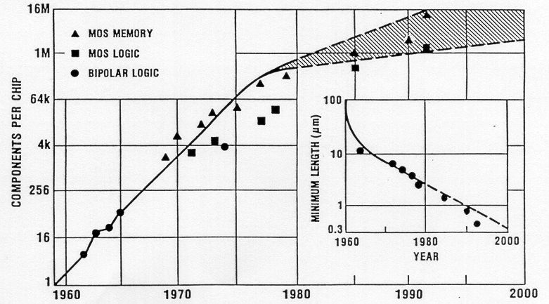
Therefore, the current trend of integration will also continue in the foreseeable future. Advances in device manufacturing technology, and especially the steady reduction of minimum feature size (minimum length of a transistor or an interconnect realizable on chip) support this trend. Figure 1.2 shows the history and forecast of chip complexity - and minimum feature size - over time, as seen in the early 1980s. At that time, a minimum feature size of 0.3 microns was expected around the year 2000. The actual development of the technology, however, has far exceeded these expectations. A minimum size of 0.25 microns was readily achievable by the year 1995. As a direct result of this, the integration density has also exceeded previous expectations - the first 64 Mbit DRAM, and the INTEL Pentium microprocessor chip containing more than 3 million transistors were already available by 1994, pushing the envelope of integration density.
When comparing the integration density of integrated circuits, a clear distinction must be made between the memory chips and logic chips. Figure 1.3 shows the level of integration over time for memory and logic chips, starting in 1970. It can be observed that in terms of transistor count, logic chips contain significantly fewer transistors in any given year mainly due to large consumption of chip area for complex interconnects. Memory circuits are highly regular and thus more cells can be integrated with much less area for interconnects.
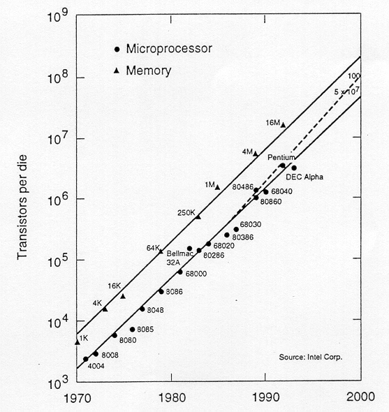
Generally speaking, logic chips such as microprocessor chips and digital signal processing (DSP) chips contain not only large arrays of memory (SRAM) cells, but also many different functional units. As a result, their design complexity is considered much higher than that of memory chips, although advanced memory chips contain some sophisticated logic functions. The design complexity of logic chips increases almost exponentially with the number of transistors to be integrated. This is translated into the increase in the design cycle time, which is the time period from the start of the chip development until the mask-tape delivery time. However, in order to make the best use of the current technology, the chip development time has to be short enough to allow the maturing of chip manufacturing and timely delivery to customers. As a result, the level of actual logic integration tends to fall short of the integration level achievable with the current processing technology. Sophisticated computer-aided design (CAD) tools and methodologies are developed and applied in order to manage the rapidly increasing design complexity.
The design process, at various levels, is usually evolutionary in nature. It starts with a given set of requirements. Initial design is developed and tested against the requirements. When requirements are not met, the design has to be improved. If such improvement is either not possible or too costly, then the revision of requirements and its impact analysis must be considered. The Y-chart (first introduced by D. Gajski) shown in Fig. 1.4 illustrates a design flow for most logic chips, using design activities on three different axes (domains) which resemble the letter Y.

The Y-chart consists of three major domains, namely:
The design flow starts from the algorithm that describes the behavior of the target chip. The corresponding architecture of the processor is first defined. It is mapped onto the chip surface by floorplanning. The next design evolution in the behavioral domain defines finite state machines (FSMs) which are structurally implemented with functional modules such as registers and arithmetic logic units (ALUs). These modules are then geometrically placed onto the chip surface using CAD tools for automatic module placement followed by routing, with a goal of minimizing the interconnects area and signal delays. The third evolution starts with a behavioral module description. Individual modules are then implemented with leaf cells. At this stage the chip is described in terms of logic gates (leaf cells), which can be placed and interconnected by using a cell placement & routing program. The last evolution involves a detailed Boolean description of leaf cells followed by a transistor level implementation of leaf cells and mask generation. In standard-cell based design, leaf cells are already pre-designed and stored in a library for logic design use.

Figure 1.5 provides a more simplified view of the VLSI design flow, taking into account the various representations, or abstractions of design - behavioral, logic, circuit and mask layout. Note that the verification of design plays a very important role in every step during this process. The failure to properly verify a design in its early phases typically causes significant and expensive re-design at a later stage, which ultimately increases the time-to-market.
Although the design process has been described in linear fashion for simplicity, in reality there are many iterations back and forth, especially between any two neighboring steps, and occasionally even remotely separated pairs. Although top-down design flow provides an excellent design process control, in reality, there is no truly unidirectional top-down design flow. Both top-down and bottom-up approaches have to be combined. For instance, if a chip designer defined an architecture without close estimation of the corresponding chip area, then it is very likely that the resulting chip layout exceeds the area limit of the available technology. In such a case, in order to fit the architecture into the allowable chip area, some functions may have to be removed and the design process must be repeated. Such changes may require significant modification of the original requirements. Thus, it is very important to feed forward low-level information to higher levels (bottom up) as early as possible.
In the following, we will examine design methodologies and structured approaches which have been developed over the years to deal with both complex hardware and software projects. Regardless of the actual size of the project, the basic principles of structured design will improve the prospects of success. Some of the classical techniques for reducing the complexity of IC design are: Hierarchy, regularity, modularity and locality.
The use of hierarchy, or �divide and conquer� technique involves dividing a module into sub- modules and then repeating this operation on the sub-modules until the complexity of the smaller parts becomes manageable. This approach is very similar to the software case where large programs are split into smaller and smaller sections until simple subroutines, with well-defined functions and interfaces, can be written. In Section 1.2, we have seen that the design of a VLSI chip can be represented in three domains. Correspondingly, a hierarchy structure can be described in each domain separately. However, it is important for the simplicity of design that the hierarchies in different domains can be mapped into each other easily.
As an example of structural hierarchy, Fig. 1.6 shows the structural decomposition of a CMOS four-bit adder into its components. The adder can be decomposed progressively into one- bit adders, separate carry and sum circuits, and finally, into individual logic gates. At this lower level of the hierarchy, the design of a simple circuit realizing a well-defined Boolean function is much more easier to handle than at the higher levels of the hierarchy.
In the physical domain, partitioning a complex system into its various functional blocks will provide a valuable guidance for the actual realization of these blocks on chip. Obviously, the approximate shape and size (area) of each sub-module should be estimated in order to provide a useful floorplan. Figure 1.7 shows the hierarchical decomposition of a four-bit adder in physical description (geometrical layout) domain, resulting in a simple floorplan. This physical view describes the external geometry of the adder, the locations of input and output pins, and how pin locations allow some signals (in this case the carry signals) to be transferred from one sub-block to the other without external routing. At lower levels of the physical hierarchy, the internal mask

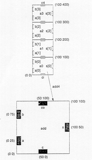
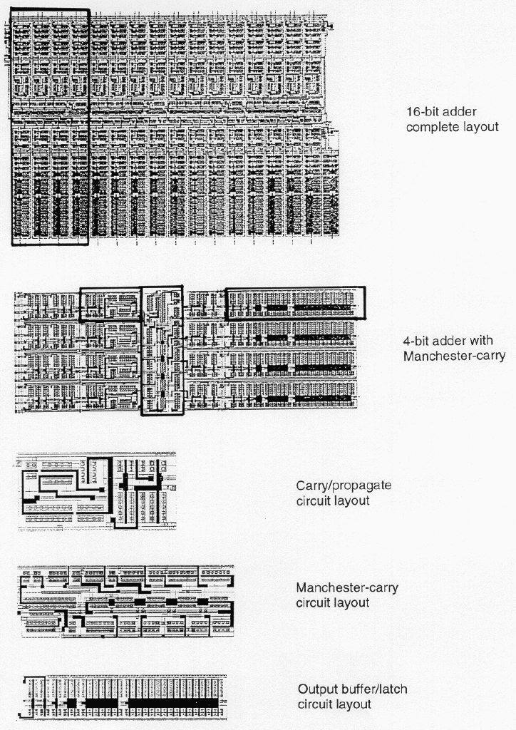

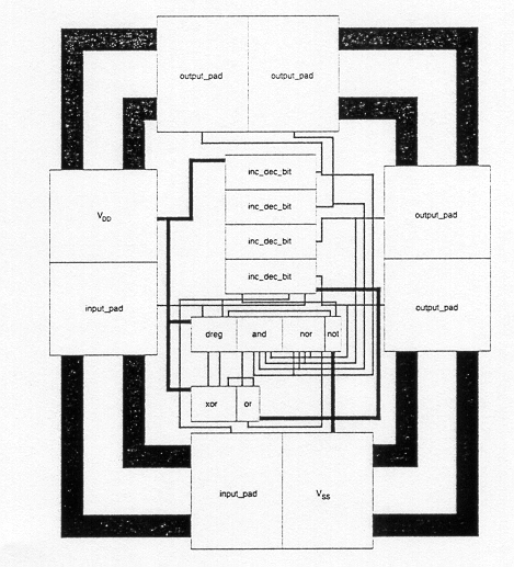
layout of each adder cell defines the locations and the connections of each transistor and wire. Figure 1.8 shows the full-custom layout of a 16-bit dynamic CMOS adder, and the sub-modules that describe the lower levels of its physical hierarchy. Here, the 16-bit adder consists of a cascade connection of four 4-bit adders, and each 4-bit adder can again be decomposed into its functional blocks such as the Manchester chain, carry/propagate circuits and the output buffers. Finally, Fig. 1.9 and Fig. 1.10 show the structural hierarchy and the physical layout of a simple triangle generator chip, respectively. Note that there is a corresponding physical description for every module in the structural hierarchy, i.e., the components of the physical view closely match this structural view.
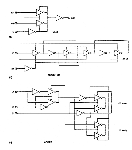
The hierarchical design approach reduces the design complexity by dividing the large system into several sub-modules. Usually, other design concepts and design approaches are also needed to simplify the process. Regularity means that the hierarchical decomposition of a large system should result in not only simple, but also similar blocks, as much as possible. A good example of regularity is the design of array structures consisting of identical cells - such as a parallel multiplication array. Regularity can exist at all levels of abstraction: At the transistor level, uniformly sized transistors simplify the design. At the logic level, identical gate structures can be used, etc. Figure 1.11 shows regular circuit-level designs of a 2-1 MUX (multiplexer), an D-type edge-triggered flip flop, and a one-bit full adder. Note that all of these circuits were designed by using inverters and tri-state buffers only. If the designer has a small library of well-defined and well-characterized basic building blocks, a number of different functions can be constructed by using this principle. Regularity usually reduces the number of different modules that need to be designed and verified, at all levels of abstraction.
Modularity in design means that the various functional blocks which make up the larger system must have well-defined functions and interfaces. Modularity allows that each block or module can be designed relatively independently from each other, since there is no ambiguity about the function and the signal interface of these blocks. All of the blocks can be combined with ease at the end of the design process, to form the large system. The concept of modularity enables the parallelisation of the design process. It also allows the use of generic modules in various designs - the well-defined functionality and signal interface allow plug-and-play design.
By defining well-characterized interfaces for each module in the system, we effectively ensure that the internals of each module become unimportant to the exterior modules. Internal details remain at the local level. The concept of locality also ensures that connections are mostly between neighboring modules, avoiding long-distance connections as much as possible. This last point is extremely important for avoiding excessive interconnect delays. Time-critical operations should be performed locally, without the need to access distant modules or signals. If necessary, the replication of some logic may solve this problem in large system architectures.
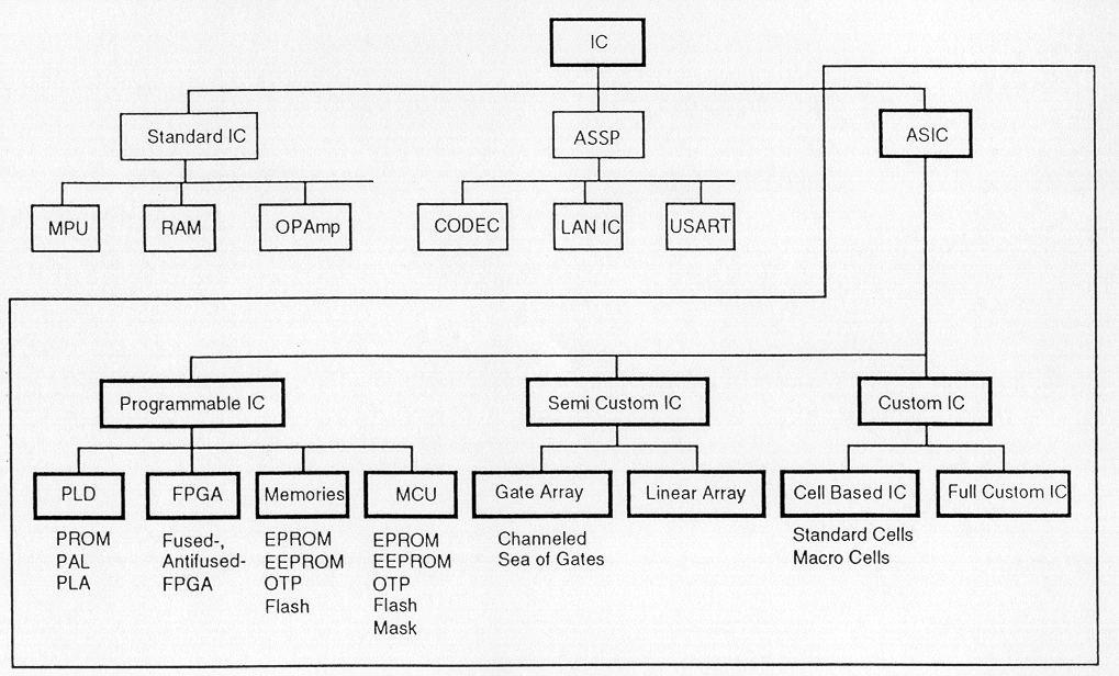
Several design styles can be considered for chip implementation of specified algorithms or logic functions. Each design style has its own merits and shortcomings, and thus a proper choice has to be made by designers in order to provide the functionality at low cost.
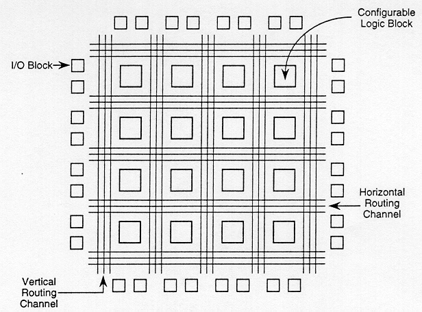
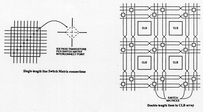
Fully fabricated FPGA chips containing thousands of logic gates or even more, with programmable interconnects, are available to users for their custom hardware programming to realize desired functionality. This design style provides a means for fast prototyping and also for cost-effective chip design, especially for low-volume applications. A typical field programmable gate array (FPGA) chip consists of I/O buffers, an array of configurable logic blocks (CLBs), and programmable interconnect structures. The programming of the interconnects is implemented by programming of RAM cells whose output terminals are connected to the gates of MOS pass transistors. A general architecture of FPGA from XILINX is shown in Fig. 1.12. A more detailed view showing the locations of switch matrices used for interconnect routing is given in Fig. 1.13.
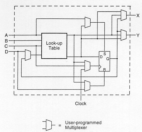
A simple CLB (model XC2000 from XILINX) is shown in Fig. 1.14. It consists of four signal input terminals (A, B, C, D), a clock signal terminal, user-programmable multiplexers, an SR-latch, and a look-up table (LUT). The LUT is a digital memory that stores the truth table of the Boolean function. Thus, it can generate any function of up to four variables or any two functions of three variables. The control terminals of multiplexers are not shown explicitly in Fig. 1.14.
The CLB is configured such that many different logic functions can be realized by programming its array. More sophisticated CLBs have also been introduced to map complex functions. The typical design flow of an FPGA chip starts with the behavioral description of its functionality, using a hardware description language such as VHDL. The synthesized architecture is then technology-mapped (or partitioned) into circuits or logic cells. At this stage, the chip design is completely described in terms of available logic cells. Next, the placement and routing step assigns individual logic cells to FPGA sites (CLBs) and determines the routing patterns among the cells in accordance with the netlist. After routing is completed, the on-chip
performance of the design can be simulated and verified before downloading the design for programming of the FPGA chip. The programming of the chip remains valid as long as the chip is powered-on, or until new programming is done. In most cases, full utilization of the FPGA chip area is not possible - many cell sites may remain unused.
The largest advantage of FPGA-based design is the very short turn-around time, i.e., the time required from the start of the design process until a functional chip is available. Since no physical manufacturing step is necessary for customizing the FPGA chip, a functional sample can be obtained almost as soon as the design is mapped into a specific technology. The typical price of FPGA chips are usually higher than other realization alternatives (such as gate array or standard cells) of the same design, but for small-volume production of ASIC chips and for fast prototyping, FPGA offers a very valuable option.
In view of the fast prototyping capability, the gate array (GA) comes after the FPGA. While the design implementation of the FPGA chip is done with user programming, that of the gate array is done with metal mask design and processing. Gate array implementation requires a two-step manufacturing process: The first phase, which is based on generic (standard) masks, results in an array of uncommitted transistors on each GA chip. These uncommitted chips can be stored for later customization, which is completed by defining the metal interconnects between the transistors of the array (Fig. 1.15). Since the patterning of metallic interconnects is done at the end of the chip fabrication, the turn-around time can be still short, a few days to a few weeks. Figure 1.16 shows a corner of a gate array chip which contains bonding pads on its left and bottom edges, diodes for I/O protection, nMOS transistors and pMOS transistors for chip output driver circuits in the neighboring areas of bonding pads, arrays of nMOS transistors and pMOS transistors, underpass wire segments, and power and ground buses along with contact windows.


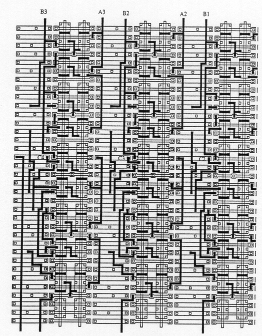
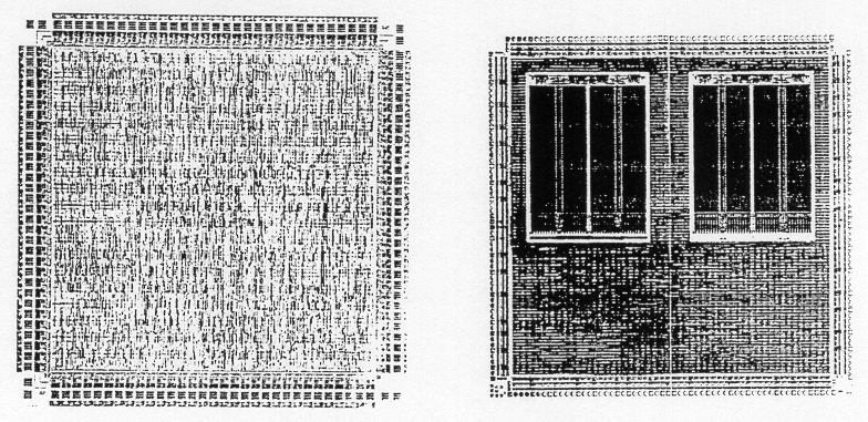
Figure 1.17 shows a magnified portion of the internal array with metal mask design (metal lines highlighted in dark) to realize a complex logic function. Typical gate array platforms allow dedicated areas, called channels, for intercell routing as shown in Figs. 1.16 and 1.17 between rows or columns of MOS transistors. The availability of these routing channels simplifies the interconnections, even using one metal layer only. The interconnection patterns to realize basic logic gates can be stored in a library, which can then be used to customize rows of uncommitted transistors according to the netlist. While most gate array platforms only contain rows of uncommitted transistors separated by routing channels, some other platforms also offer dedicated memory (RAM) arrays to allow a higher density where memory functions are required. Figure 1.18 shows the layout views of a conventional gate array and a gate array platform with two dedicated memory banks.
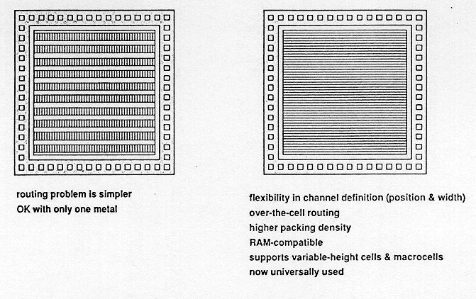
With the use of multiple interconnect layers, the routing can be achieved over the active cell areas; thus, the routing channels can be removed as in Sea-of-Gates (SOG) chips. Here, the entire chip surface is covered with uncommitted nMOS and pMOS transistors. As in the gate array case, neighboring transistors can be customized using a metal mask to form basic logic gates. For intercell routing, however, some of the uncommitted transistors must be sacrificed. This approach results in more flexibility for interconnections, and usually in a higher density. The basic platform of a SOG chip is shown in Fig. 1.19. Figure 1.20 offers a brief comparison between the channeled (GA) vs. the channelless (SOG) approaches.

In general, the GA chip utilization factor, as measured by the used chip area divided by the total chip area, is higher than that of the FPGA and so is the chip speed, since more customized design can be achieved with metal mask designs. The current gate array chips can implement as many as hundreds of thousands of logic gates.
The standard-cells based design is one of the most prevalent full custom design styles which require development of a full custom mask set. The standard cell is also called the polycell. In this design style, all of the commonly used logic cells are developed, characterized, and stored in a standard cell library. A typical library may contain a few hundred cells including inverters, NAND gates, NOR gates, complex AOI, OAI gates, D-latches, and flip-flops. Each gate type can have multiple implementations to provide adequate driving capability for different fanouts. For instance, the inverter gate can have standard size transistors, double size transistors, and quadruple size transistors so that the chip designer can choose the proper size to achieve high circuit speed and layout density. The characterization of each cell is done for several different categories. It consists of
To enable automated placement of the cells and routing of inter-cell connections, each cell layout is designed with a fixed height, so that a number of cells can be abutted side-by-side to form rows. The power and ground rails typically run parallel to the upper and lower boundaries of the cell, thus, neighboring cells share a common power and ground bus. The input and output pins are located on the upper and lower boundaries of the cell. Figure 1.21 shows the layout of a typical standard cell. Notice that the nMOS transistors are located closer to the ground rail while the pMOS transistors are placed closer to the power rail.
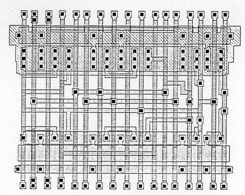
Figure 1.22 shows a floorplan for standard-cell based design. Inside the I/O frame which is reserved for I/O cells, the chip area contains rows or columns of standard cells. Between cell rows are channels for dedicated inter-cell routing. As in the case of Sea-of-Gates, with over-the- cell routing, the channel areas can be reduced or even removed provided that the cell rows offer sufficient routing space. The physical design and layout of logic cells ensure that when cells are placed into rows, their heights are matched and neighboring cells can be abutted side-by-side, which provides natural connections for power and ground lines in each row. The signal delay, noise margins, and power consumption of each cell should be also optimized with proper sizing of transistors using circuit simulation.
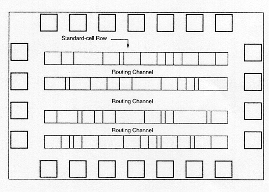
If a number of cells must share the same input and/or output signals, a common signal bus structure can also be incorporated into the standard-cell-based chip layout. Figure 1.23 shows the simplified symbolic view of a case where a signal bus has been inserted between the rows of standard cells. Note that in this case the chip consists of two blocks, and power/ground routing must be provided from both sides of the layout area. Standard-cell based designs may consist of several such macro-blocks, each corresponding to a specific unit of the system architecture such as ALU, control logic, etc.
After chip logic design is done using standard cells in the library, the most challenging task is to place individual cells into rows and interconnect them in a way that meets stringent design goals in circuit speed, chip area, and power consumption. Many advanced CAD tools for place-and-route have been developed and used to achieve such goals. Also from the chip layout, circuit models which include interconnect parasitics can be extracted and used for timing simulation and analysis to identify timing critical paths. For timing critical paths, proper gate sizing is often practiced to meet the timing requirements. In many VLSI chips, such as microprocessors and digital signal processing chips, standard-cells based design is used to implement complex control logic modules. Some full custom chips can be also implemented exclusively with standard cells.
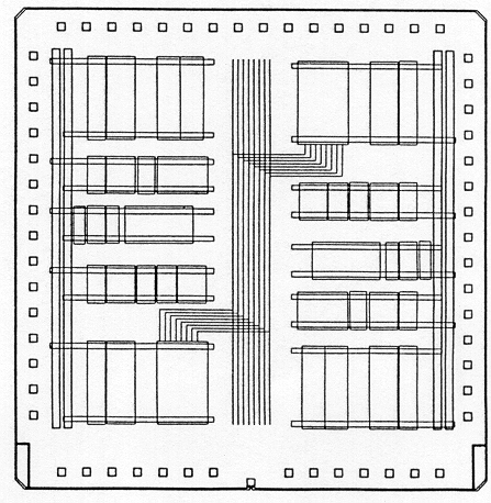
Finally, Fig. 1.24 shows the detailed mask layout of a standard-cell-based chip with an uninterrupted single block of cell rows, and three memory banks placed on one side of the chip. Notice that within the cell block, the separations between neighboring rows depend on the number of wires in the routing channel between the cell rows. If a high interconnect density can be achieved in the routing channel, the standard cell rows can be placed closer to each other, resulting in a smaller chip area. The availability of dedicated memory blocks also reduces the area, since the realization of memory elements using standard cells would occupy a larger area.

Although the standard-cells based design is often called full custom design, in a strict sense, it is somewhat less than fully custom since the cells are pre-designed for general use and the same cells are utilized in many different chip designs. In a fuller custom design, the entire mask design is done anew without use of any library. However, the development cost of such a design style is becoming prohibitively high. Thus, the concept of design reuse is becoming popular in order to reduce design cycle time and development cost. The most rigorous full custom design can be the design of a memory cell, be it static or dynamic. Since the same layout design is replicated, there would not be any alternative to high density memory chip design. For logic chip design, a good compromise can be achieved by using a combination of different design styles on the same chip, such as standard cells, data-path cells and PLAs. In real full-custom layout in which the geometry, orientation and placement of every transistor is done individually by the designer, design productivity is usually very low - typically 10 to 20 transistors per day, per designer.
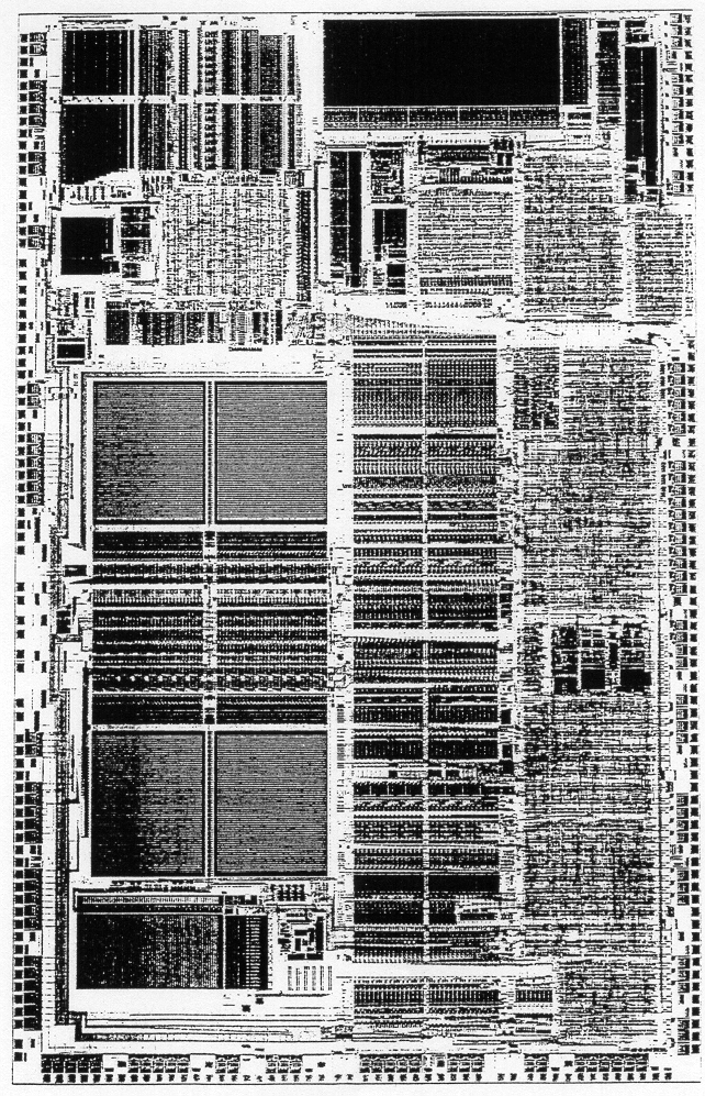
In digital CMOS VLSI, full-custom design is rarely used due to the high labor cost. Exceptions to this include the design of high-volume products such as memory chips, high- performance microprocessors and FPGA masters. Figure 1.25 shows the full layout of the Intel 486 microprocessor chip, which is a good example of a hybrid full-custom design. Here, one can identify four different design styles on one chip: Memory banks (RAM cache), data-path units consisting of bit-slice cells, control circuitry mainly consisting of standard cells and PLA blocks.
This chapter edited by Y. Leblebici
a joint production of

